Patch Antenna Ground Plane Design bbdevelopers
The ground plane provides a low-impedance path for the return current to flow, ensuring efficient voltage recovery and minimizing voltage drops or fluctuations. A multilayer PCB design with more than four layers requires more attention, so the manufacturer should use a high-quality board for the ground plane.
PCB Ground Plane Design in High Performance Boards PCB Design Blog Altium Designer
Vertical plane Characteristics Techniques v t e In electrical engineering, a ground plane is an electrically conductive surface, usually connected to electrical ground . The term has two different meanings in separate areas of electrical engineering.
2021 Detail Guide for PCB Ground Plane PCBA Store
Ground planes in a printed circuit board provide the return path for electrical current and are considered the zero-reference voltage for the design. In addition to their reference voltage, ground planes also serve many other functions in the design: Shielding
Ground Planes in Your TwoLayer PCB PCB Design Blog Altium
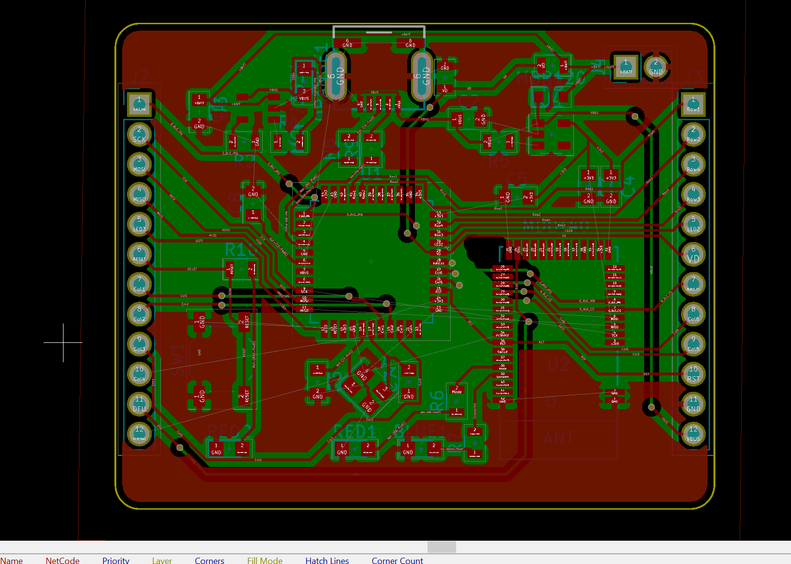
PCB design tool functionality that will help in the creation of ground planes. An internal PCB ground plane with top-mounted components and traces. My first experience debugging an electrical ground was trying to figure out why the lights on our motorcycle trailer kept blinking.

5/8 Vertical Ground Plane antenna for 10 meters IW5EDI Simone HamRadio
This keeps loop inductance small and ensures low EMI emission, which is a major reason to use a ground plane or grounded copper pour in a multilayer PCB stackup. EMI shielding and suppression: EMI goes both ways, and grounded copper in your design can provide shielding against external sources of EMI. Decoupling and stable power: This is.

PPT PCB Design & Layout Tips PowerPoint Presentation ID219082
A PCB ground plane is important in PCB design and manufacturing. Also, designers use a power or ground plane in multilayer stackups. A good ground connection is necessary for great performance in a printed circuit board. A ground plane prevents electromagnetic interference in PCBs. Designing a circuit board requires an effective ground plane.
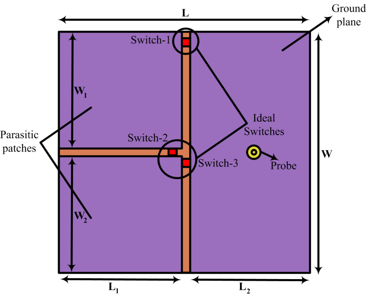
Ground plane configuration Download Scientific Diagram
The ground plane serves three important purposes in a printed circuit board: Voltage return: Most every component on the PCB will connect to a power net, and then the return voltage will come back through the ground net. On boards with only one or two layers, ground nets usually have to be routed using wider traces.
Understanding 2Layer PCB Ground Planes PCB Design Blog Altium
Published Jan. 6, 2024 Updated Jan. 8, 2024. After a portion of an Alaska Airlines Boeing 737 Max 9 jetliner's fuselage blew out in midair on Friday and caused an emergency landing in Portland.

PCB Ground Plane Best Practices in Your Multilayer Stackup Blog Altium Designer
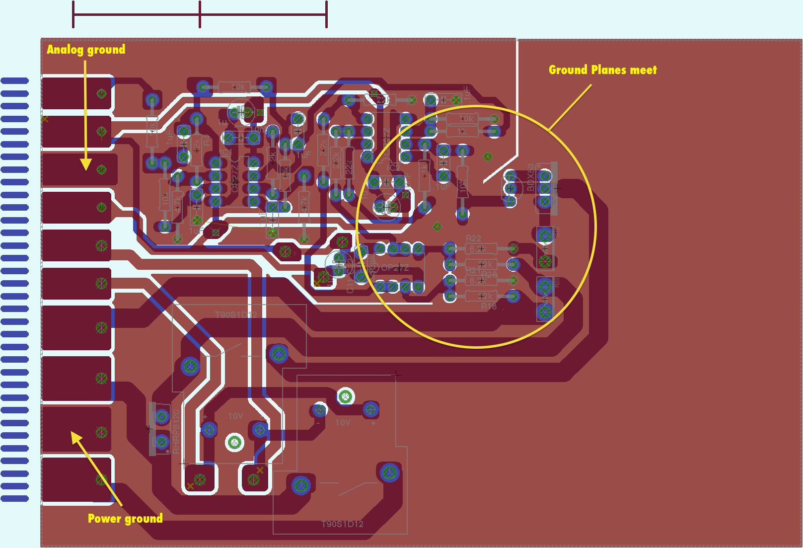
There are three PCB design guidelines that everyone loves to hate: Never route at 90-degree angles. Most "rules of thumb" involving distances and clearances between copper. Never separate analog and digital ground planes. Only the last of these design guidelines has any level of legitimacy, and it is something of a necessity in modern PCBs.

Commercial wing in ground effect plane
Simon / 2021-04-26 Contents [ hide] What Is A PCB Ground? Why is the PCB Ground Plane Important? Great PCB Grounding Techniques Top PCB Grounding Rules You Should Follow Conclusion Focusing on developing a solid foundation for your project is the key to making it succeed. Without a sturdy foundation, then the project can be subject to failure.
How to create proper ground plane Layout KiCad.info Forums
Using a ground plane is the most common technique used by many PCB designers. A ground plane, typically made of copper, covers all the areas of a PCB that do not have components or traces on them. Some rules apply for a ground plane depending on the number of layers a board has. For instance, if your board has two layers, the rules state that.

Ground Plane 5 KJ4PWP
Simpler and Smaller A ground plane improves the electrical characteristics of your circuit while also simplifying your layout task and in some cases reducing the size of your PCB. I'm not going to dwell on these aspects because I think that they're more or less self-explanatory.
PCB Ground Plane Design in High Performance Boards PCB Design Blog Altium Designer
Part of Alaska Airlines plane that blew out mid-flight found. The Federal Aviation Administration on Saturday grounded 171 of the Boeing 737 Max 9 planes worldwide so they could be inspected. On.

Creating a Ground Plane for Your PCB Design PCB Design Blog Altium
Ground Plane PCB Design Guidelines and Their Connections. The following recommendations are critical when using circuit board design tools to create ground copper planes. Routing. Route the ground layer using the widest trace for single-layer boards. And it is advisable to design the ground plane to provide electrical benefits.
AFRL Designs Tapered Ground Plane for SUAV > WrightPatterson AFB > Article Display
The first thing to do when creating an internal plane is to add a design layer specifically for the plane. In the picture below, you can see that two layers have been added as internal planes in the layer stack manager, which is found in the "Design" pulldown menu. They have been named "GND" and "PWR" respectively and occupy layers two and three.
Integrated Ground Plane Shilpa Architects
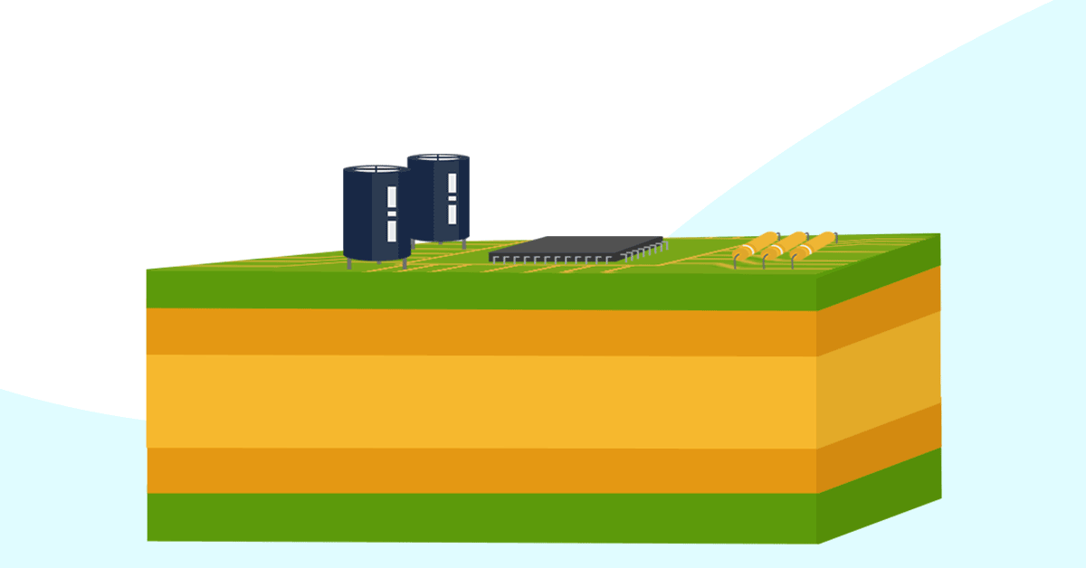
A ground plane is an essential concept in the world of electronics and electrical engineering. It pertains to a large area of copper on a Printed Circuit Board (PCB) which is connected to the circuit's ground point, typically denoted as 'GND' in circuit diagrams. Importance of Ground Planes